
VP Kamala Harris Promotes Semiconductor Research and Development in Silicon Valley
TL;DR Summary
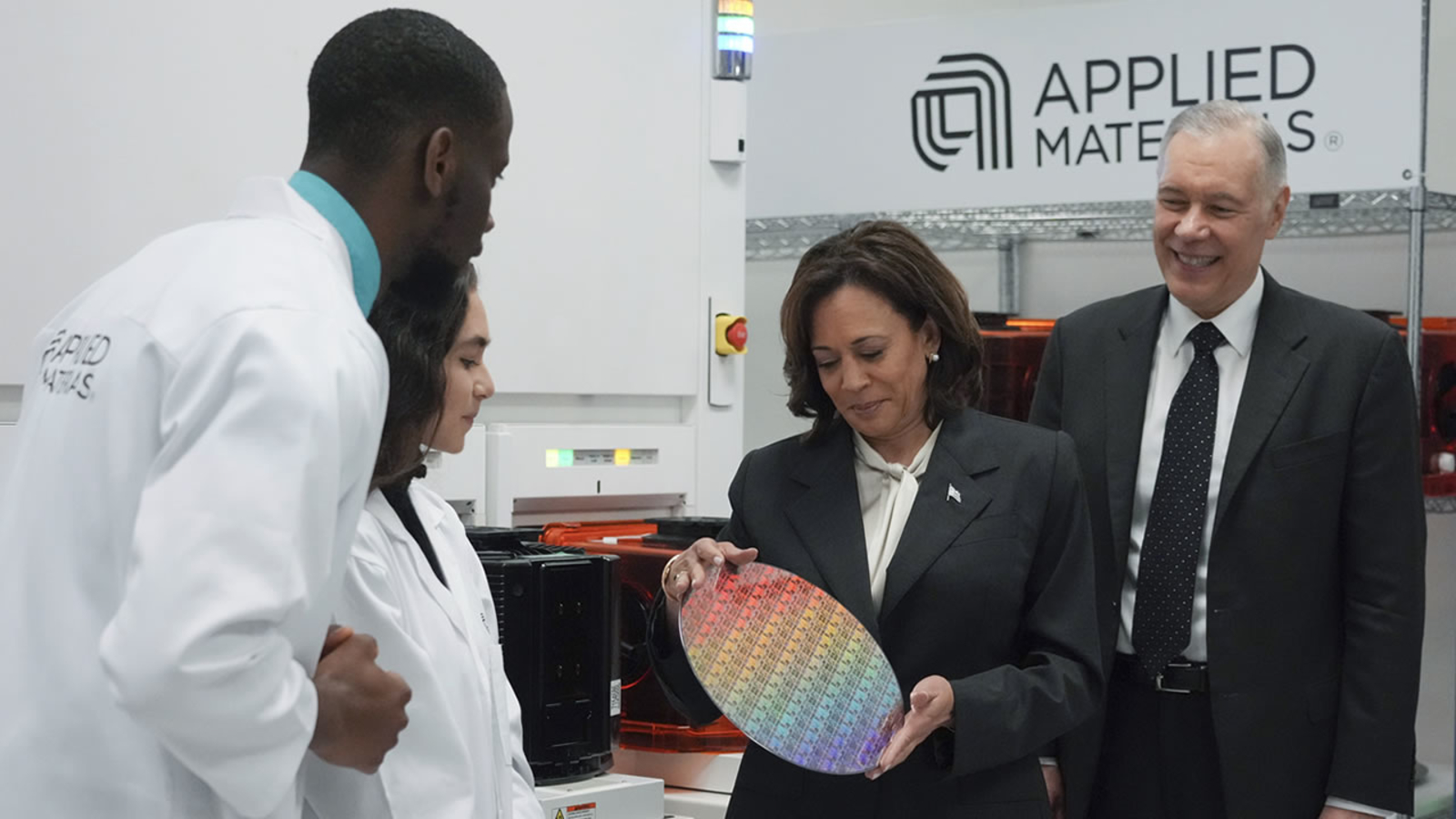
Vice President Kamala Harris announced that a new semiconductor research and development facility will be built by early 2026 in Sunnyvale's Applied Materials, which will be the largest such facility in the world. The investment of $53 billion in semiconductor research and development and manufacturing aims to encourage more production of semiconductor chips in the U.S. and maintain Silicon Valley's place as the hub of ever-evolving technology.
Topics:business#applied-materials#kamala-harris#research-and-development#semiconductor-chips#silicon-valley#technology
- World's largest semiconductor technology site being built in San Francisco Bay Area, says VP Kamala Harris KGO-TV
- A few ideas for Vice President Kamala Harris’ Sunnyvale visit The Mercury News
- VP Kamala Harris Visits Bay Area for Semiconductor Research and Development NBC Bay Area
- Kamala Harris touts launch of $4B research center in Silicon Valley San Francisco Chronicle
- Vice President Harris Delivers Remarks on the Implementation of the CHIPS and Science Act The White House
- View Full Coverage on Google News
Reading Insights
Total Reads
0
Unique Readers
8
Time Saved
2 min
vs 3 min read
Condensed
85%
462 → 67 words
Want the full story? Read the original article
Read on KGO-TV