
Optimizing SMA Connector Footprint for RF Projects.
TL;DR
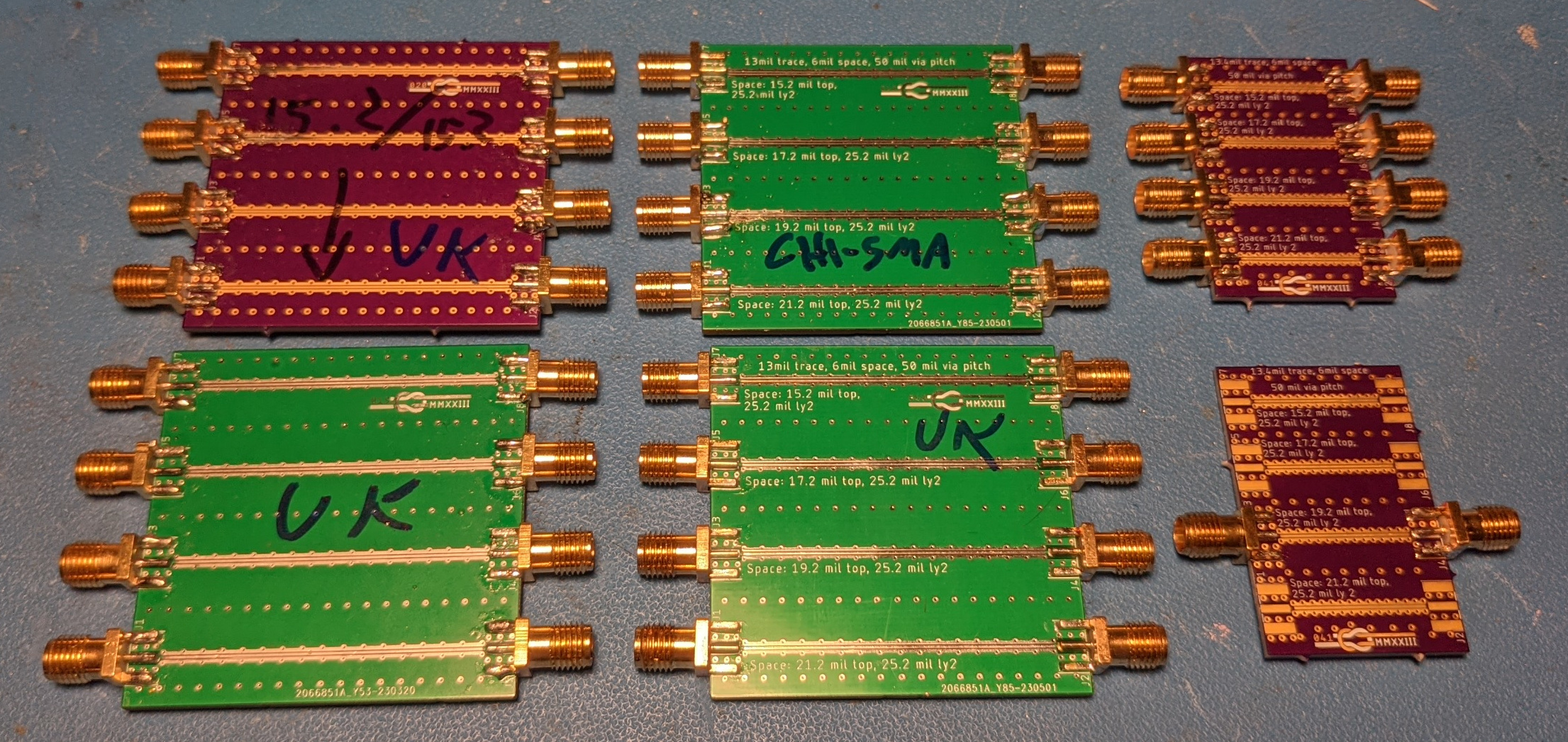
[Rob Ruark] provides tips on how to get decent performance from edge-launch SMA connections for RF applications. The first step is to lock down the PCB process via a specific stack-up. The returned PCBs were characterized using a NanoVNA V2 Plus, to get the S11 (return loss) curve up to about 4.5 GHz, confirming at about -26 dB they were already in a good position for optimization.
Topics:technologyelectronics#characteristic-impedance#edge-launch#electronics#pcb#rf-applications#sma-connector
Want the full story? Read the original reporting
Read on Hackaday