The quiet engine behind modern chips: ASML’s EUV leap
TL;DR Summary
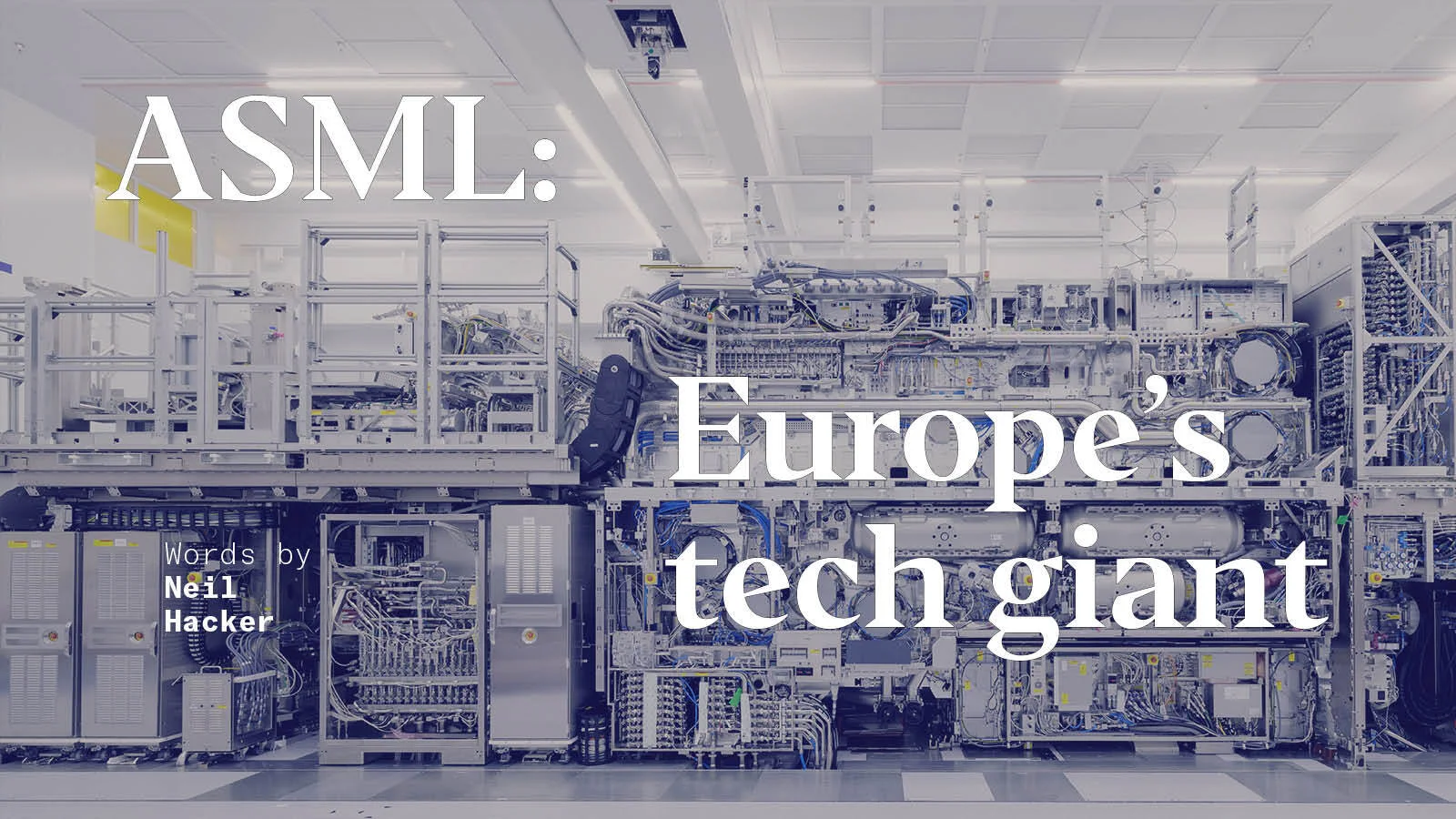
ASML’s extreme ultraviolet lithography machines—built through decades of risky R&D, strong public-private partnerships, and a vast European supplier network—are the backbone of today’s sub-5nm semiconductors. By outspending rivals, innovating with immersion lithography and the dual-stage TWINSCAN architecture, and forging tight ties with Intel, Samsung, and TSMC, ASML rose from near collapse to global dominance, reshaping the chip industry and geopolitics while pushing Moore’s Law forward toward ever-smaller transistors.
- The world’s most complex machine Works in Progress Magazine
- ASML Has Just Delivered Massive News for Micron Technology Investors The Motley Fool
- ASML Holding (ASML) Price Target Lifted by $100 Amid ‘Overdone’ Pullback Yahoo Finance
- The Race to Make the World’s Most In-Demand Machine WSJ
- ASML says firm will not be chip industry's bottleneck Reuters
Reading Insights
Total Reads
1
Unique Readers
28
Time Saved
20 min
vs 21 min read
Condensed
98%
4,124 → 68 words
Want the full story? Read the original article
Read on Works in Progress Magazine