Ski-jump photonics deliver ultra-fast, chip-to-world beam scanning with diffraction-limited beams
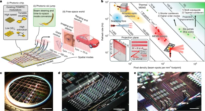
Researchers unveil a photonic ski-jump: a nanoscale waveguide monolithically integrated on a piezoelectric cantilever that curls out of a CMOS chip to emit a broadband, diffraction-limited beam. When driven near resonance, the device achieves 2D beam scanning with high efficiency, a footprint-efficient metric (up to 68.6 mega spots s–1 mm–2), and the potential to reach millions of pixels at 100 Hz from roughly a 1.5 mm footprint, outperforming MEMS by over 50×. Demonstrations include full-color image/video projection and resonant optical addressing of silicon-vacancy centers in diamond, with a 64-ski-jump array showing uniform curvature (<2% variation) and a pathway to gigaspot, kilohertz-rate scanning within a sub-5 cm diameter package. Fabricated in a CMOS-foundry, the platform promises scalable chip-to-world interfaces for LiDAR, displays, quantum information processing, and beyond, including on-chip modulation and cryogenic integration for quantum memories.