
Tag

Backside Power Delivery

All articles tagged with #backside power delivery

SemiAnalysis Teardown Reveals Intel 18A’s Backside Power and GAA Transistor Architecture
technology13 days ago

SemiAnalysis Teardown Reveals Intel 18A’s Backside Power and GAA Transistor Architecture

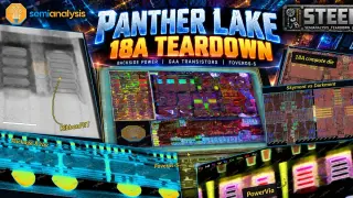
SemiAnalysis’s STEEL team has published a detailed teardown of Intel’s Panther Lake chip, marking the first commercial use of Intel’s 18A process node. The analysis confirms the implementation of backside power delivery (PowerVia) and gate-all-around (GAA) transistors, known as RibbonFETs. While the 18A logic density matches TSMC’s N3E, it does not yet surpass TSMC’s N2 or Samsung’s SF2 in peak density. The teardown highlights significant material and structural changes, including the use of molybdenum-lined tungsten contacts and a four-nanosheet transistor stack, which improves gate control but adds process complexity and thermal resistance.

Intel's PowerVia Chipmaking Tech Set to Revolutionize PC Chips in 2024.
technology3 years ago

Intel's PowerVia Chipmaking Tech Set to Revolutionize PC Chips in 2024.

Intel will present papers on their upcoming PowerVia chip fabrication technology at the annual VLSI Symposium. PowerVia and RibbonFET are set to serve as Intel’s big one-two punch to the rest of the silicon lithography industry, introducing two major chip technologies together that Intel believes will vault them back into the fab leadership position. PowerVia is Intel’s implementation of backside power delivery networks, which is seen as an essential technology to continue developing ever-finer process node technologies. Intel expects to be the first of the big three chip fabs to productize the technology, bringing it into chips at least two years ahead of its competitors.