
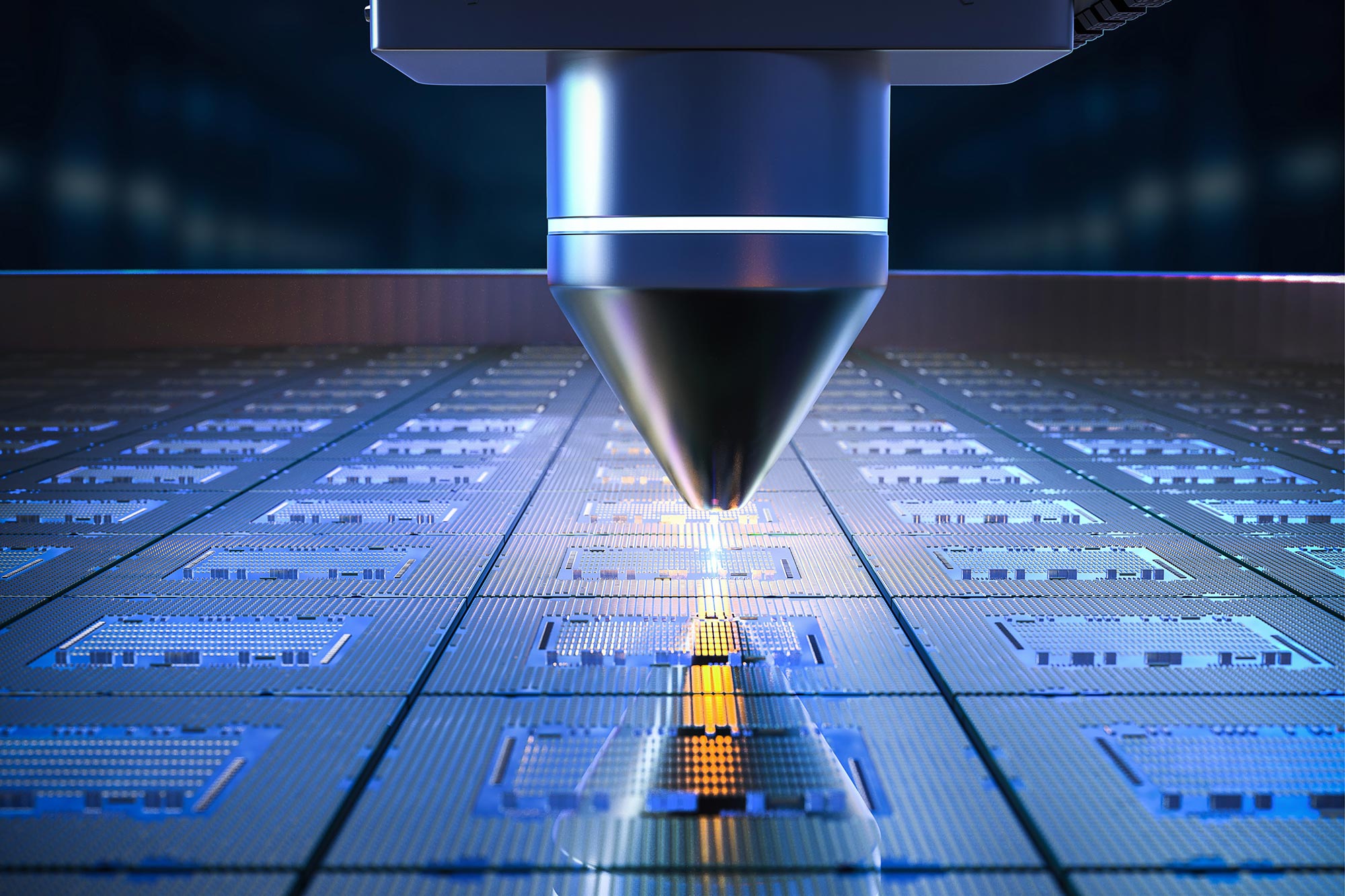
MIT Engineers Develop Atomically Thin Transistors for Super Dense Computer Chips.
MIT researchers have developed a low-temperature growth process to directly integrate 2D materials onto silicon chips, enabling denser and more powerful semiconductors. This technology bypasses previous challenges related to high temperatures and material transfer imperfections. It also reduces growth time and allows for uniform layers across larger 8-inch wafers, making it ideal for commercial applications. The new method involves growing layers of 2D transition metal dichalcogenide (TMD) materials directly on top of a silicon chip, a process that typically requires high temperatures that could damage the silicon.