
Tag

3d Packaging

All articles tagged with #3d packaging

SK Hynix Eyes 3D HBM Leap With EMIB, Hybrid Bonding and 2 TB/s Bandwidth
technology2 days ago

SK Hynix Eyes 3D HBM Leap With EMIB, Hybrid Bonding and 2 TB/s Bandwidth

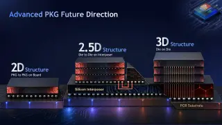
SK Hynix outlined a plan to push high-bandwidth memory (HBM) into true 3D stacking by adopting advanced packaging like Intel EMIB and hybrid bonding, aiming to go beyond 16-Hi stacks. Its HBM4 roadmap targets up to 24 Gb per DRAM die, up to 36 GB per stack, 2,048 IOs, up to 8 Gbps per IO, and around 2 TB/s bandwidth, with higher stacks and more TSVs; the company is optimizing packaging tradeoffs (MR+MUF vs TC+NCF) to address warpage, gap fill, power, and thermal challenges, while envisioning 3D integration that stacks HBM on accelerators and potential Intel collaboration.

AMD CEO Lisa Su Talks Future of Moore's Law and Chip Technology
technology3 years ago

AMD CEO Lisa Su Talks Future of Moore's Law and Chip Technology

AMD CEO, Dr. Lisa Su, states that Moore's Law is not dead but has slowed down and things need to be done differently to overcome the performance, efficiency, and cost challenges. AMD has been the pioneer of advancing 3D packaging and chiplet technology with its first HBM designs back in 2015, chiplet processors in 2017, and also the first 3D packaging on a chip with its 3D V-Cache design in 2022. AMD is already working with 3nm as of right now and that they are also looking at 2nm and beyond that.