
New Etching Flux Method Enables Deterministic Nucleation for 2D Semiconductor Integration
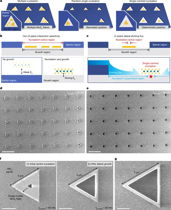
Researchers have developed a new method to control where 2D semiconductor crystals begin to form, enabling precise single-crystal growth and advanced device integration.
Key points
- A new technique called etching-flux-mediated single-centred nucleation (EF-SCN) allows for deterministic placement of a single crystal nucleus at the center of a growth region.
- The method uses oxygen released from a hafnium oxide barrier to suppress nucleation near edges, leaving only the center viable for crystal growth.
- This approach enables the growth of large single-crystal molybdenum disulfide flakes up to 10 micrometers in size with high uniformity.
- The technique supports low-temperature processing at 430 degrees Celsius using zirconium dioxide barriers, enhancing compatibility with existing semiconductor manufacturing.
- EF-SCN facilitates the creation of complex structures, including multiple transistors within a single crystal and self-aligned contacts for lateral heterostructures.
Background
This development builds on previous efforts in area-selective growth (ASG) for 2D transition-metal dichalcogenides (TMDs), which previously struggled with stochastic nucleation that limited crystal size and uniformity. While ASG could confine deposition to specific regions, it could not control the exact position of individual nuclei within those regions. The new EF-SCN method addresses this limitation by introducing in-plane spatial control through chemical fluxes, moving beyond traditional out-of-plane selectivity. This advancement is significant for the broader goal of integrating 2D materials into advanced electronic devices, where precise crystal placement is critical for performance and yield.
Why it matters
Precise control over crystal nucleation is essential for scaling up 2D semiconductor production and improving device performance. By enabling deterministic single-crystal growth, this method reduces variability in electronic properties, such as field-effect mobility, and allows for the integration of multiple functional components within a single crystal. This could lead to more efficient and reliable 2D electronic devices, potentially impacting the development of next-generation transistors and integrated circuits.
What to watch
Researchers will likely explore the application of EF-SCN to other 2D materials and device architectures. Further studies may focus on optimizing the process for even lower temperatures and larger-scale manufacturing. Additionally, the development of new device configurations, such as self-aligned contacts and lateral heterostructures, will be tested for practical applications in electronic integration.
Want the full story? Read the original reporting
Read on Nature