Tag

Two Dimensional Materials

All articles tagged with #two dimensional materials

Light-Driven Polarons Reveal a Wigner Crystal in a 2D WSe2 Monolayer
science18 days ago

Light-Driven Polarons Reveal a Wigner Crystal in a 2D WSe2 Monolayer

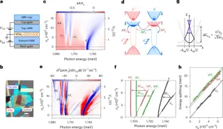
A cryogenic, gate-tunable WSe2 monolayer hosts a robust Wigner crystal whose collective excitations dress excitons into light–matter polarons. The researchers observe two WP resonances that blueshift with electron density due to hybridization with WC excitations and Bragg-umklapp scattering, alongside exciton-umklapp features. WP intensities depend on the WC spin state and can be controlled magnetically or optically with circular polarization, enabling an optical interface to the electron crystal’s spin. A simple hybridization model captures the density-dependent AP–WP splitting, linking WC dynamics to observable optical spectra. This work demonstrates a versatile platform for studying strongly correlated order via hybrid light–matter excitations in 2D materials and suggests ways to probe WC gaps and spin phenomena optically.

Picometer-precision atom steering yields mesoscopic defect crystal in CrSBr
science3 months ago

Picometer-precision atom steering yields mesoscopic defect crystal in CrSBr

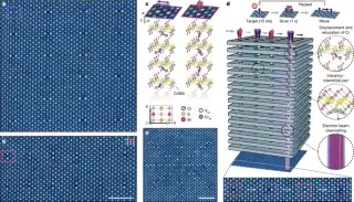
Researchers demonstrate deterministic atomic engineering inside CrSBr by steering Cr atoms with sub-20-pm accuracy to create a mesoscopic 3D defect crystal (~40,000 defects) within a 150×100×13 nm volume. The engineered lattice is stable at room temperature and opens routes for deterministic colour-centre placement, quantum simulations of many-body systems, and scalable atomic-scale manufacturing outside the microscope.

Residue-Free Field Effect Transistors: Pioneering Beyond-Silicon Technology
technology3 years ago

Residue-Free Field Effect Transistors: Pioneering Beyond-Silicon Technology

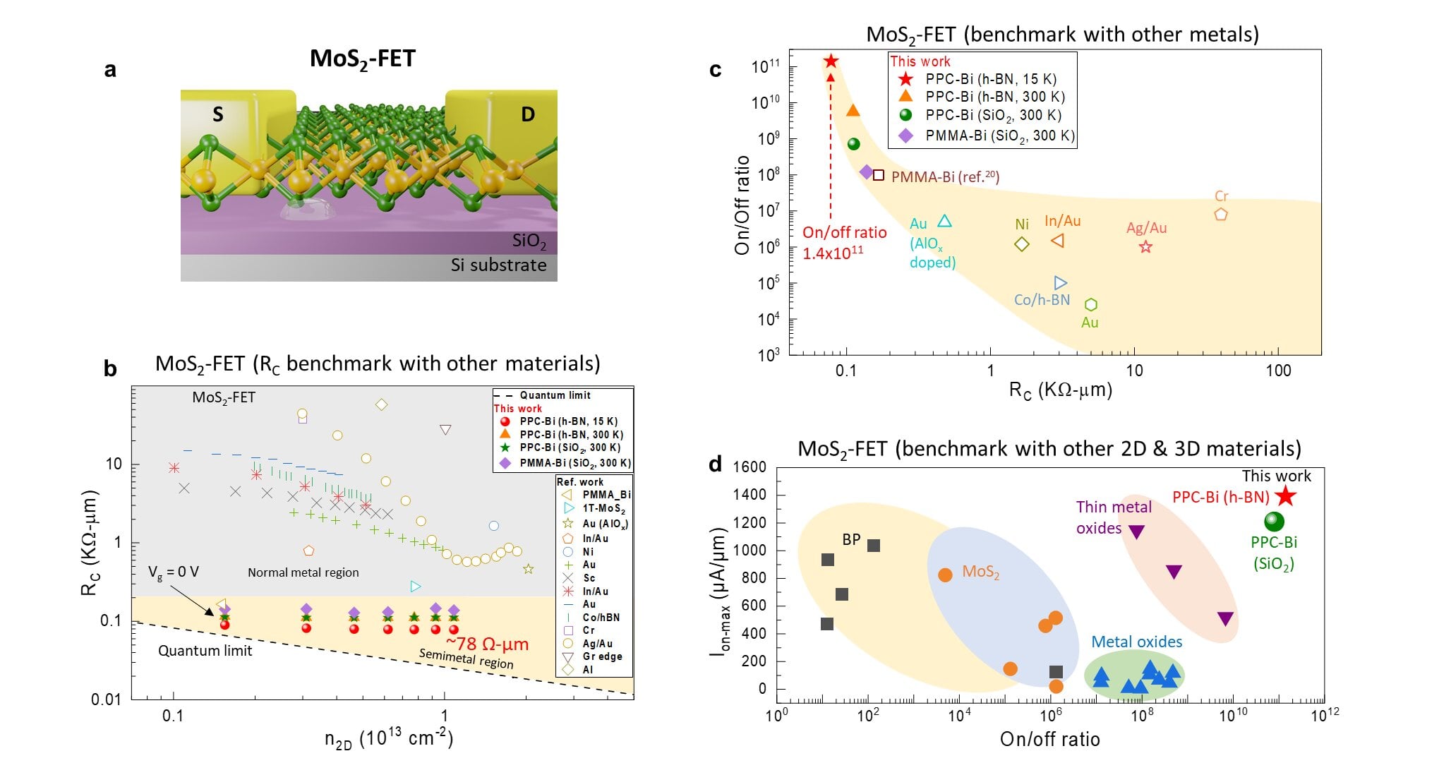
Researchers from the Institute for Basic Science in South Korea have made a breakthrough in the fabrication of field-effect transistors (FET) by successfully using polypropylene carbonate (PPC) for residue-free wet transfer. This method allows for the production of wafer-scale two-dimensional transition metal dichalcogenides (TMDs) without the introduction of residues or wrinkles. The FET device built using this technique exhibited high electrical performance, surpassing previously reported values. The researchers believe that this technology can be easily implemented using existing integrated circuit manufacturing processes, opening up possibilities for beyond-silicon-based semiconductor technologies.

"Nanoclays: Revolutionizing Chemists' Toolbox with Innovative Additions"
science-and-technology3 years ago

"Nanoclays: Revolutionizing Chemists' Toolbox with Innovative Additions"

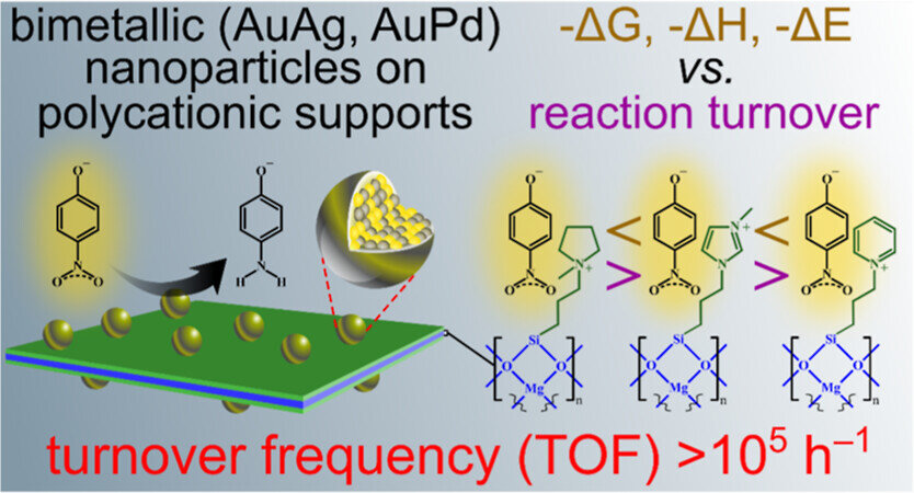
Researchers at the University of Missouri have developed nanoclays, microscopic materials made of clay, that have electrically charged surfaces and can be customized with different chemical components. These nanoclays can be used in various applications, such as biomedical imaging, environmental science, and explosive detection. The two-dimensional nature of nanoclays allows them to coat objects with thin layers, introducing different surface properties. The researchers believe that nanoclays have immense potential for creating new chemical building blocks with specific functions.

"Breakthrough: Scientists Successfully Construct Monoatomic Lead Layers Using Innovative Method"
science-and-technology3 years ago

"Breakthrough: Scientists Successfully Construct Monoatomic Lead Layers Using Innovative Method"

Researchers have developed a method for synthesizing and analyzing two-dimensional lead layers, providing a comprehensive understanding of their structures. The controlled coupling of functionalized graphene to these lead layers opens up possibilities for investigating and controlling correlation effects and mesoscopic phenomena in 2D materials, such as superconductivity and novel magnetic phases. The research has implications for the development of electronic systems and quantum materials for quantum computing.

Visualizing Quantum States in 2D Materials
science-and-technology3 years ago

Visualizing Quantum States in 2D Materials

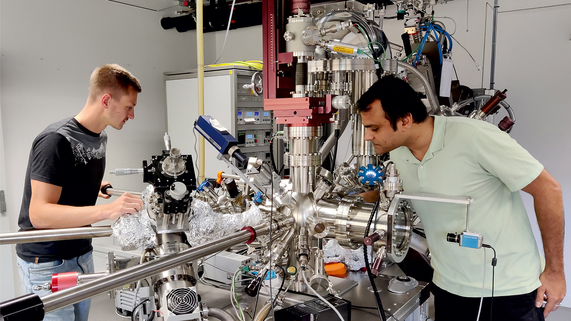
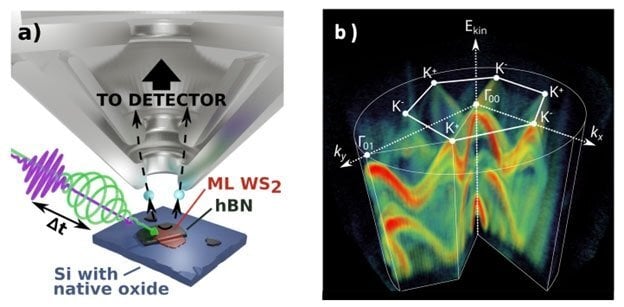
Scientists have developed a new approach to create separate images of individual quantum states in two-dimensional crystals of tungsten disulfide (WS2) using a technique called time-resolved momentum microscopy. By tracking the individual quantum states, researchers showed that the coupling mechanisms that lead to mixing of the states may not fully match current theories. This study provides crucial experimental support for some current theories of exciton coupling in TMDs, but also sheds light on important discrepancies.